- 您现在的位置:买卖IC网 > Sheet目录325 > FAN7384MX (Fairchild Semiconductor)IC DRIVER GATE HALF BRIDGE 14SOP
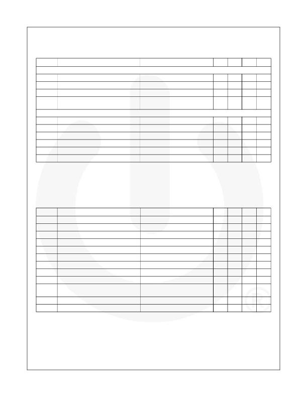
Electrical Characteristics (Continued)
V BIAS (V DD , V BS ) = 15.0V, T A = 25 ? C, unless otherwise specified. The V IN and I IN parameters are referenced to GND.
The V O and I O parameters are referenced to GND and V S is applicable to HO and LO.
Symbol
Characteristics
Condition
Min. Typ. Max. Unit
SHORT-CIRCUIT PROTECTION
V CSCREF Short-circuit detector reference voltage
0.47
0.50
0.53
V
I CSCIN
I SOFT
-V CSC
Short-circuit input current
Soft turn-off source current
Negative CSC pin immunity (5)
V CSCIN =1V, R CSCIN =100K ?
V DD =15V
Voltage on CSC pin up to -12V,
Time<2 ? s
5
5
10
10
15
15
-20
? A
mA
V
FAULT DETECTION SECTION
V FINH
V FINL
Fault input high level voltage
Fault input low level voltage
2.5
1.2
V
V
V FINHYS
Fault input hysteresis
voltage (5)
0.5
V
V FOH
V FOL
Fault output high level voltage
Fault output low level voltage
V CSC =0V, R PULL-UP =4.7K ?
V CSC =1V, I FO =2mA
4.7
0.8
V
V
t FO
Fault output pulse width
V CSCIN =1V
60
100
μs
Note:
5. These parameters guaranteed by design.
Dynamic Electrical Characteristics
T A =25 ? C, V BIAS (V DD , V BS ) = 15.0V, V S = GND, C Load = 1000pF unless otherwise specified.
Symbol
Parameter
Conditions
Min. Typ. Max. Unit
t on
t off
t r
t f
MT
DT
t UVFLT
t CSCFLT
t CSCFO
Turn-on propagation delay
Turn-off propagation delay
Turn-on rise time
Turn-off fall time
Delay matching
Dead-time
Under-voltage filtering time (5)
time (5)
CSC pin filtering
FO (5)
Time from CSC triggering to
V S =0V
V S =0V or 600V (5)
80
180
170
50
30
120
16
300
350
260
240
100
80
50
170
ns
ns
ns
ns
ns
ns
μs
ns
ns
t CSCLO
t SDFO
Time from CSC triggering to low-side From V CSC =1V to starting gate
gate output (5) turn-off
Shutdown to FO propagation delay (5)
600
60
ns
ns
t SDOFF
Shutdown to HIGH/LOW-side gate
off (5)
100
ns
Note:
5. These parameters guaranteed by design.
? 2006 Fairchild Semiconductor Corporation
FAN7384 Rev. 1.0.8
7
www.fairchildsemi.com
发布紧急采购,3分钟左右您将得到回复。
相关PDF资料
FAN7385MX
IC GATE DRIVER HISIDE 2CH 14-SOP
FAN7388MX
IC GATE DRIVER HALF BRIDG 20SOIC
FAN73892MX
IC GATE DVR HALF BRDG 3PH 28SOIC
FAN7389MX
IC GATE-DRIVE 3PH HALFBRDG 24SOP
FAN73901M
IC GATE DRIVER HI/LOW SIDE 8SOIC
FAN7390M1X
IC DRIVER GATE HI/LO SIDE 14-SOP
FAN7392N
IC GATE DVR MONO HI/LO 14DIP
FAN73932M
IC GATE DVR HALF BRIDGE 8-SOIC
相关代理商/技术参数
FAN7385
制造商:FAIRCHILD 制造商全称:Fairchild Semiconductor 功能描述:Dual-Channel High-Side Gate-Drive IC
FAN7385M
功能描述:功率驱动器IC 2-Ch High Side Only Gate Driver RoHS:否 制造商:Micrel 产品:MOSFET Gate Drivers 类型:Low Cost High or Low Side MOSFET Driver 上升时间: 下降时间: 电源电压-最大:30 V 电源电压-最小:2.75 V 电源电流: 最大功率耗散: 最大工作温度:+ 85 C 安装风格:SMD/SMT 封装 / 箱体:SOIC-8 封装:Tube
FAN7385MX
功能描述:功率驱动器IC 2Ch High Side Only Gate Driver RoHS:否 制造商:Micrel 产品:MOSFET Gate Drivers 类型:Low Cost High or Low Side MOSFET Driver 上升时间: 下降时间: 电源电压-最大:30 V 电源电压-最小:2.75 V 电源电流: 最大功率耗散: 最大工作温度:+ 85 C 安装风格:SMD/SMT 封装 / 箱体:SOIC-8 封装:Tube
FAN7387
制造商:Rochester Electronics LLC 功能描述: 制造商:Fairchild Semiconductor Corporation 功能描述:
FAN7387M
功能描述:功率驱动器IC Half-Bridge Gate Driver RoHS:否 制造商:Micrel 产品:MOSFET Gate Drivers 类型:Low Cost High or Low Side MOSFET Driver 上升时间: 下降时间: 电源电压-最大:30 V 电源电压-最小:2.75 V 电源电流: 最大功率耗散: 最大工作温度:+ 85 C 安装风格:SMD/SMT 封装 / 箱体:SOIC-8 封装:Tube
FAN7387MX
功能描述:功率驱动器IC Half Bridge Gate 600V 25mA .625W RoHS:否 制造商:Micrel 产品:MOSFET Gate Drivers 类型:Low Cost High or Low Side MOSFET Driver 上升时间: 下降时间: 电源电压-最大:30 V 电源电压-最小:2.75 V 电源电流: 最大功率耗散: 最大工作温度:+ 85 C 安装风格:SMD/SMT 封装 / 箱体:SOIC-8 封装:Tube
FAN7387N
功能描述:功率驱动器IC Half Bridge Gate 600V 25mA 1.2W RoHS:否 制造商:Micrel 产品:MOSFET Gate Drivers 类型:Low Cost High or Low Side MOSFET Driver 上升时间: 下降时间: 电源电压-最大:30 V 电源电压-最小:2.75 V 电源电流: 最大功率耗散: 最大工作温度:+ 85 C 安装风格:SMD/SMT 封装 / 箱体:SOIC-8 封装:Tube
FAN7387V
制造商:FAIRCHILD 制造商全称:Fairchild Semiconductor 功能描述:Ballast Control IC for Compact Fluorescent Lamp
